MMBF4416LT1�
� http://onsemi.com�
� 6�
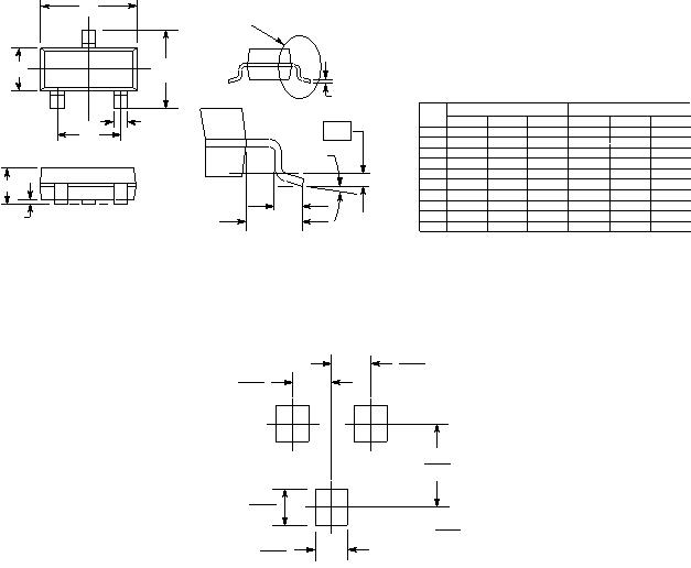
� PACKAGE DIMENSIONS�
� SOT?23 (TO?236)�
� CASE 318?08�
� ISSUE AN�
� D�
� A1�
� 3�
� 12�
� NOTES:�
� 1. DIMENSIONING AND TOLERANCING PER ANSI�
� Y14.5M, 1982.�
� 2. CONTROLLING DIMENSION: INCH.�
� 3. MAXIMUM LEAD THICKNESS INCLUDES LEAD�
� FINISH THICKNESS. MINIMUM LEAD�
� THICKNESS IS THE MINIMUM THICKNESS OF�
� BASE MATERIAL.�
� 4. 318?01 THRU ?07 AND ?09 OBSOLETE, NEW�
� STANDARD 318?08.�
� SCALE 10:1�
� �
� mm�
� inches�
� 0.8�
� 0.031�
� 0.9�
� 0.035�
� 0.95�
� 0.037�
� 0.95�
� 0.037�
� 2.0�
� 0.079�
� VIEW C�
� L�
� 0.25�
� L1�
� �
� e�
� E�
� HE�
� b�
� A�
� SEE VIEW C�
� DIM�
� A�
� MIN NOM MAX MIN�
� MILLIMETERS�
� 0.89 1.00 1.11 0.035�
� INCHES�
� A1�
� 0.01 0.06 0.10 0.001�
� b�
� 0.37 0.44 0.50 0.015�
� c�
� 0.09 0.13 0.18 0.003�
� D�
� 2.80 2.90 3.04 0.110�
� E�
� 1.20 1.30 1.40 0.047�
� e�
� 1.78 1.90 2.04 0.070�
� L�
� 0.10 0.20 0.30 0.004�
� 0.040 0.044�
� 0.002 0.004�
� 0.018 0.020�
� 0.005 0.007�
� 0.114 0.120�
� 0.051 0.055�
� 0.075 0.081�
� 0.008 0.012�
� NOM MAX�
� L1�
� 2.10 2.40 2.64 0.083�
� 0.094 0.104�
� HE�
� 0.35 0.54 0.69 0.014 0.021 0.029�
� c�
� *For additional information on our Pb?Free strategy and soldering�
� details, please download the ON Semiconductor Soldering and�
� Mounting Techniques Reference Manual, SOLDERRM/D.�
� SOLDERING FOOTPRINT*�
� STYLE 10:�
� PIN 1. DRAIN�
� 2. SOURCE�
� 3. GATE�
� ON Semiconductor�
� and are registered trademarks of Semiconductor Components Industries, LLC (SCILLC). SCILLC reserves the right to mak�
� e changes without further notice�
� to any products herein. SCILLC makes no warranty, representation or guarantee regarding the suitability of its products for any particular purpose, nor does SCILLC assume any liability�
� arising out of the application or use of any product or circuit, and specifically disclaims any and all liability, including without limitation special, consequential or incidental damages.�
� “Typical” parameters which may be provided in SCILLC data sheets and/or specifications can and do vary in different applications and actual performance may vary over time. All�
� operating parameters, including “Typicals” must be validated for each customer application by customer’s technical experts. SCILLC does not convey any license under its patent rights�
� nor the rights of others. SCILLC products are not designed, intended, or authorized for use as components in systems intended for surgical implant into the body, or other applications�
� intended to support or sustain life, or for any other application in which the failure of the SCILLC product could create a situation where personal injury or death may occur. Should�
� Buyer purchase or use SCILLC products for any such unintended or unauthorized application, Buyer shall indemnify and hold SCILLC and its officers, employees, subsidiaries, affiliates,�
� and distributors harmless against all claims, costs, damages, and expenses, and reasonable attorney fees arising out of, directly or indirectly, any claim of personal injury or death�
� associated with such unintended or unauthorized use, even if such claim alleges that SCILLC was negligent regarding the design or manufacture of the part. SCILLC is an Equal�
� Opportunity/Affirmative Action Employer. This literature is subject to all applicable copyright laws and is not for resale in any manner.�
� PUBLICATION ORDERING INFORMATION�
� N. American Technical Support: 800?282?9855 Toll Free�
� USA/Canada�
� : 480?829?7710 or 800?344?3860 Toll Free USA/Canada�
� Japan: ON Semiconductor, Japan Customer Focus Center�
� 2?9?1 Kamimeguro, Meguro?ku, Tokyo, Japan 153?0051�
� Phone: 81?3?5773?3850�
� MMBF4416LT1/D�
� LITERATURE FULFILLMENT:�
� Literature Distribution Center for ON Semiconductor�
� P.O. Box 61312, Phoenix, Arizona 85082?1312 USA�
� Phone�
� Fax: 480?829?7709 or 800?344?3867�
� Toll Free USA/Canada�
� Email: orderlit@onsemi.com�
� ON Semiconductor Website: http://onsemi.com�
� Order Literature: http://www.onsemi.com/litorder�
� For additional information, please contact your�
� local Sales Representative.�
�  �
�
� � �  �
�
� � �  �
�
� � �  �
�
� � 发布紧急采购,3分钟左右您将得到回复。
相关PDF资料
MMBF4416
IC AMP RF N-CHANNEL SOT-23
MMBFJ309LT1G
JFET SS N-CHAN 25V SOT23
MMBFJ310
IC SWITCH RF N-CH 25V 10MA SOT23
MMBV3401LT1
DIODE TUNING SS 35V SOT23
MMBV3700LT1G
DIODE TUNING SS 200V SOT23
MMDL101T1
DIODE SCHOTTKY 7V 200MW SOD-323
MMDL301T1
DIODE SCHOTTKY 200MW 30V SOD-323
MMVL3401T1
DIODE PIN SWITCHING 35V SOD-323
相关代理商/技术参数
MMBF4416LT1G
制造商:ON Semiconductor 功能描述:TRANSISTORJFETN-Channel30V V(BR)DSS5
MMBF5103
功能描述:JFET N-Ch amplifier Lo Freq/Lo Noise RoHS:否 制造商:ON Semiconductor 晶体管极性:N-Channel 漏极电流(Vgs=0 时的 Idss):50 mA 漏源电压 VDS:15 V 闸/源击穿电压: 漏极连续电流:50 mA 配置: 安装风格: 封装 / 箱体:SC-59 封装:Reel
MMBF5103_Q
功能描述:JFET N-Ch amplifier Lo Freq/Lo Noise
RoHS:否 制造商:ON Semiconductor 晶体管极性:N-Channel 漏极电流(Vgs=0 时的 Idss):50 mA 漏源电压 VDS:15 V 闸/源击穿电压: 漏极连续电流:50 mA 配置: 安装风格: 封装 / 箱体:SC-59 封装:Reel
MMBF5434
功能描述:JFET N-Channel Switch RoHS:否 制造商:ON Semiconductor 晶体管极性:N-Channel 漏极电流(Vgs=0 时的 Idss):50 mA 漏源电压 VDS:15 V 闸/源击穿电压: 漏极连续电流:50 mA 配置: 安装风格: 封装 / 箱体:SC-59 封装:Reel
MMBF5434_Q
功能描述:JFET N-Channel Switch
RoHS:否 制造商:ON Semiconductor 晶体管极性:N-Channel 漏极电流(Vgs=0 时的 Idss):50 mA 漏源电压 VDS:15 V 闸/源击穿电压: 漏极连续电流:50 mA 配置: 安装风格: 封装 / 箱体:SC-59 封装:Reel
MMBF5457
功能描述:JFET N-Channel Transistor General Purpose RoHS:否 制造商:ON Semiconductor 晶体管极性:N-Channel 漏极电流(Vgs=0 时的 Idss):50 mA 漏源电压 VDS:15 V 闸/源击穿电压: 漏极连续电流:50 mA 配置: 安装风格: 封装 / 箱体:SC-59 封装:Reel
MMBF5457_Q
功能描述:JFET N-Channel Transistor General Purpose
RoHS:否 制造商:ON Semiconductor 晶体管极性:N-Channel 漏极电流(Vgs=0 时的 Idss):50 mA 漏源电压 VDS:15 V 闸/源击穿电压: 漏极连续电流:50 mA 配置: 安装风格: 封装 / 箱体:SC-59 封装:Reel
MMBF5457LT1
功能描述:JFET 25V 10mA RoHS:否 制造商:ON Semiconductor 晶体管极性:N-Channel 漏极电流(Vgs=0 时的 Idss):50 mA 漏源电压 VDS:15 V 闸/源击穿电压: 漏极连续电流:50 mA 配置: 安装风格: 封装 / 箱体:SC-59 封装:Reel